
India's first experiential semiconductor learning ecosystem — real equipment, virtual fabs and AI training, brought to every school and college.
Built for students, teachers and the simply curious — three immersive simulations, each a full experience of its own.
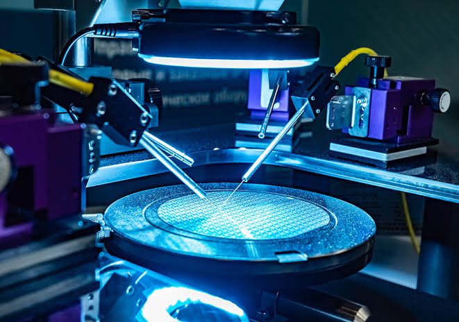
Follow a wafer through all eight stages of chip manufacturing — lithography to test — fully animated, step by step.
Enter the fab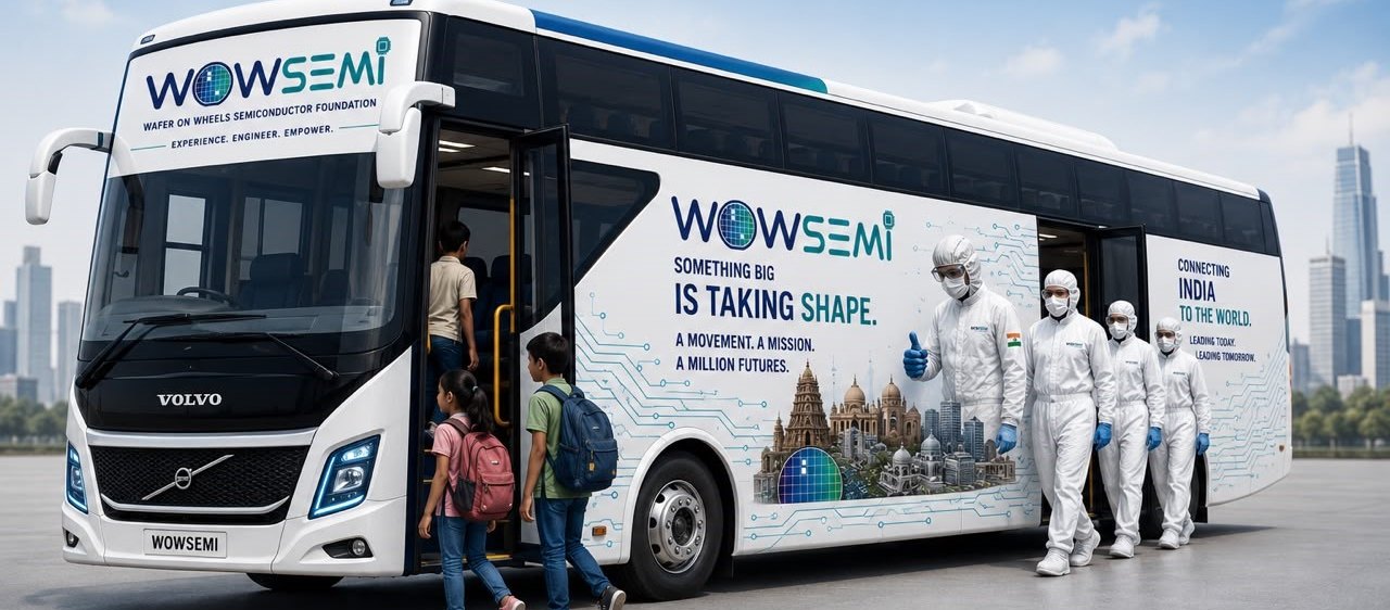
Tour the Wafer-on-Wheels bus — six learning zones of real equipment, AR/VR and a rolling semiconductor museum.
Board the bus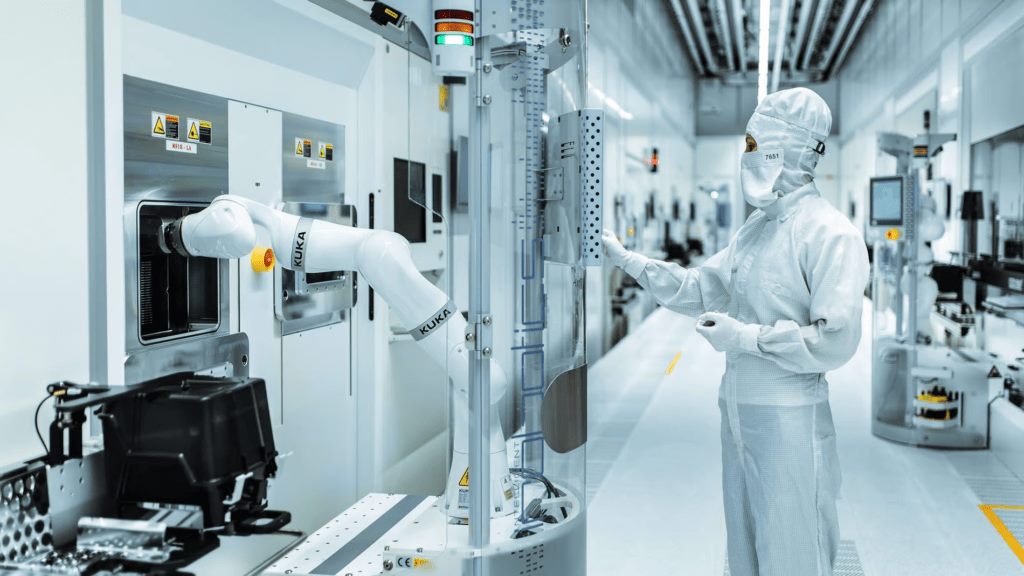
Gown up in the right order, control your particle cloud, and learn why fabs are the cleanest places on Earth.
Suit upIndia's fabs are hiring — but most graduates have never touched a wafer. WOWSemi closes that gap with one philosophy: “Experience Before Expertise.”
Not another training organization — a complete semiconductor ecosystem.
Three verbs. One pipeline. Every WOWSemi program moves a learner from first touch to industry-ready professional.
Learn by interacting with the real thing — semiconductor wafers, IC packages, MEMS devices, sensors, equipment components and cleanroom concepts, brought directly to you.
Build practical depth through equipment demonstrations, virtual fabs, AI simulators, assembly exercises, manufacturing workflows and real failure-analysis case studies.
Convert skill into opportunity — career guidance, industry mentoring, internships, innovation programs, startup incubation and entrepreneurship exposure.
It all begins with quartz sand — silicon dioxide, one of the most abundant materials on Earth. Mined, crushed and refined in an arc furnace into metallurgical-grade silicon.
District by district, with published metrics at every phase — here's the plan.
We can't hand a student a fab. We can hand them the three things that actually kill hardware startups before they begin.
Put a WOWSemi lab on the road for a year — your branding on the bus, your engineers as guest mentors, quarterly impact reports on your desk.
Sponsor a bus →Fund awareness drives, faculty training and student workshops across an entire district — measurable, named, and yours.
Adopt a district →Back certification scholarships for talented students and fab-grade lab setups on partner campuses.
Endow a scholarship →Funded through direct grants, philanthropy and co-established CSR programmes. How we structure funding →
Wafer demos, equipment miniatures, AR/VR and a rolling semiconductor museum — at your gate.
Explore the busIndustry-oriented certification — fundamentals to failure analysis, cleanroom to yield.
View levelsTrain-the-trainer, industry immersion, lab-setup guidance and classroom-ready teaching resources.
CollaborateStudents solve real industry problems — automation, AI, process optimization, sustainability.
Try a challengeSelf-paced courses, interactive simulations, virtual fab tours and AI learning assistants.
Preview a moduleThe Semiuseum — a world-class physical museum rising at our HQ, with real equipment in six halls.
Enter the SemiuseumCareer explorers, AI advisors, mentoring and internship pathways into every fab function.
Explore careersSimulate lithography, etch and yield — break things safely before touching a real tool.
Enter the fabProgressive, industry-aligned levels. Every course maps to a real fab role and counts toward a WOWSemi certificate.
First cohorts begin 1 December 2026. Levels 01–04 are WOWSemi's own ladder, not NSQF levels — certificates are issued by WOWSemi Foundation and are not NSQF-certified. What our certificate is — and is not →
A fab is a city of professions. Pick a role to see the work, the skills and the salary band — entry to senior.
Eighty years of silicon in one scrolling timeline — gold markers are the plot twists.
Bardeen, Brattain & Shockley at Bell Labs replace vacuum tubes with a sliver of germanium. Electronics is reborn.
Jack Kilby demonstrates the first IC at Texas Instruments; Robert Noyce's planar version at Fairchild soon makes it manufacturable.
Gordon Moore predicts transistor counts will double every year — revised to every two years in 1975. The industry turns it into a schedule.
The first commercial microprocessor: 2,300 transistors at 10µm. Your phone now carries billions.
Morris Chang separates design from manufacturing — enabling fabless companies and today's global chip economy.
Design centres bloom in Bengaluru, Hyderabad and Noida — India becomes a global VLSI design powerhouse.
After decades of R&D, ASML's EUV machines — printing with 13.5nm light — enter high-volume chip production.
₹76,000 crore national program launches — India commits to making chips, not just designing them.
Dholera, Sanand, Morigaon — India's first commercial fab and ATMP projects break ground and ramp.
India targets a $100B+ semiconductor economy. The engineers who build it are in classrooms today — WOWSemi is how they get ready.
Responsibility is part of the curriculum, not a footnote: Reuse. Refurb. Renew. Recycle.
A fab can use millions of litres a day — learners study reclaim, recycling and zero-liquid-discharge design.
From tool idle-mode strategies to renewable-powered plants — efficiency as an engineering discipline.
Legacy tools refurbished and redeployed — the same machines that once built chips now build engineers.
Where chips end matters as much as where they begin — responsible electronics lifecycle management.
No single actor can build a semiconductor workforce. WOWSemi runs on a five-way partnership — and the fifth leg is the one most programs leave out.
Talk to us early and we will work with your compliance team to structure the engagement correctly. Our full registration status →
Community leaders who know how to reach students, and semiconductor veterans who know what fabs actually need — working the same mission.
Whether you're a curious student, a college principal, a fab HR head or a CSR leader — there's a seat on the bus.
HQ · WOWSemi, R-28-C1B, Kovaipudur, Coimbatore - 641042, India · ☎ +91 90803 25242